|
AFM AND RELATED MICROSCOPY
This article is no longer updated since september 2007. For a recent update, please go the Néel Institute !
I. SCANNING GATE MICROSCOPY OF A QUANTUM RING We have carried out low-temperature Scanning Gate Microscopy (SGM) measurements on semiconductor quantum rings (QRs) in a magnetic field using the cryogenic AFM developped in our lab and briefly described below (part II). The electrically-polarized AFM tip is scanned over the surface, both inside and outside the quantum structure, with the ultimate goal of mapping in real space its electron transport propreties and possibly building an image of the wavefunction of the coherent electron system. Our QRs have been patterned from a high-mobility 2DEG (GaInAs heterostructure) buried close to the sample surface (25 nm) to ensure an efficient coupling with the AFM tip. They have typical outer (inner) diameters of 650 (200) nm. GaInAs has been chosen because it has favorable coherence length scales for electron transport at low temperature (Hackens et al., PRL 94, 146802 (2005)). Our measurements are performed at 4.2 K and in a magnetic field up to 6 T. Aharonov-Bohm (AB) oscillations are seen in the QR magnetoconductance as a clear signature for the contribution of coherent effects. The SGM images reveal striking oscillations of the conductance both inside and
outside the ring as the tip scans over the surface:
see images on our welcome page. Inside the ring, these
oscillations follow the QR radial symmetry with a characteristic
length of 100 nm much larger than the Fermi wavelength (25 nm). Outside the ring, the SGM images
also exhibit oscillations, but they are concentric with the ring. A detailed
analysis of the conductance maps as a function of relevant experimental
parameters (e.g. tip voltage) allows us to discriminate clearly between coherent
contributions, related to electron interferences inside the ring, and ballistic
contributions, due to billiard ball-like trajectories of the electrons within
the QR. In particular, we have shown that the concentric fringes outside the ring are
from a coherent origin and form a real-space image of the AB effect. II. Electric Force Microscopy (EFM)
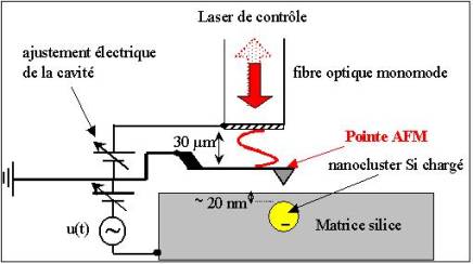
The
main goal of this project is the local electric coupling of an AFM tip (see
figure)
with
electric charges in semiconductor nanostructures in order to detect
and study their spatial distribution, down to a single electron, and to possibly
manipulate them with the tip. In
nanostructures that are burried at a few nm depth below the free surface
and that are subjected to a very low bias during the electric measurements, it
is mandatory to work at low temperature (4.2K) in a non-contact mode with a very
good force sensitivity (< 1 pN ; 1 pN= 10-12 newton, that is
the magnitude of the Coulomb interaction between two elementary charges located
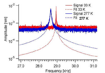
at 15 nm apart). In this context, we have developped (collaboration with J. Chevrier et F. Marchi, LEPES, CNRS Grenoble) a low-temperature AFM along the lines of the instrument developped by K. Karrai at the University of Munich (see M. Vogel et al., Appl. Phys. Lett. 78, 2592 (2001)). In this AFM, the cantilever deflection is measured by means of a Perot-Fabry microcavity that can be electrically or piezoelectrically tuned. This allows to work at low temperature, thereby reducing the thermal noise on the cantilever, and to adjust the force sensitivity by tuning the cavity length. As a result, the force sensitivity has been measured at 2 fN.(Hz)-1/2 at 33 K by analysing the thermal noise, see figure below. |
  |